Author: Ted Yapo / Source: Hackaday

You may have heard the phrase “flip-chip” before: it’s a broad term referring to several integrated circuit packaging methods, the common thread being that the semiconductor die is flipped upside down so the active surface is closest to the PCB. As opposed to the more traditional method in which the IC is face-up and connected to the packaging with bond wires, this allows for ultimate packaging efficiency and impressive performance gains.
We hear a lot about advances in the integrated circuits themselves, but the packages that carry them and the issues they solve — and sometimes create — get less exposure.
Let’s have a look at why semiconductor manufacturers decided to turn things on their head, and see how radioactive solder and ancient Roman shipwrecks fit in.
The Old Packages

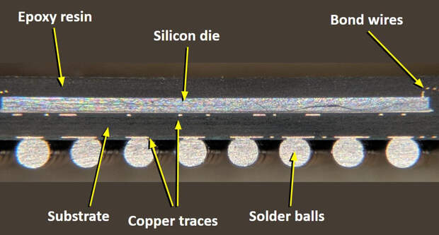
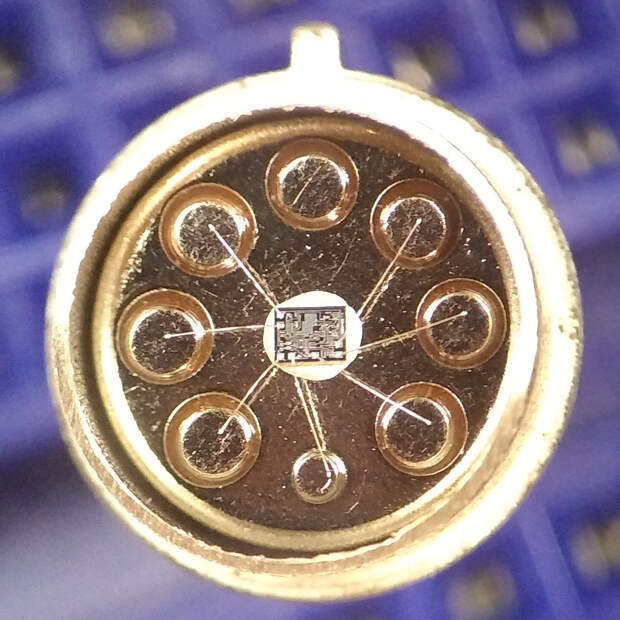
Very early integrated circuits were packaged in metal cans like the transistors of the day. Welded gold bond wires connected the die to the external pins. Open one of these old IC packages like a can of tuna, and the wires are plain to see. When DIP packages came about, they continued to use bond wires to connect the die to the IC pins, even though they were encapsulated in the plastic package.
This trend continued into surface-mount packages like SOIC, SSOP, and even BGAs, because it worked pretty well for parts from that period. But, as IC technology advanced, these packages became problematic. The first snag was the burgeoning size and complexity of the chips. As they grew, so did the number of connections required.
Unfortunately, while the complexity grows with chip area, the number of possible wire-bond connections grows with the perimeter of both the die and the old-style packages. It’sX2 vs X, and at some point, there just isn’t enough space on the perimeter, so a more dense connection method had to be devised. A second problem was the performance of the wire bonds themselves. Like any conductor in free space, these little wires behave as inductors. This inductance can have serious consequences for high-speed circuits. As IC speeds increased, the inductance of the bond wires plus that of the package leads started to become a serious issue. Flip Chips

A good solution to both problems is to turn the semiconductor die upside down. With the chip flipped this way, the connections can be made directly from the chip to the next layer below without any bond wires. This allows for more connections, since bond pads can be placed anywhere; there’s no need to restrict them to the periphery of the die. For pad-limited designs with many I/O connections, this can actually result in a smaller chip. Additionally, the connections can be made with a short, thick metallic bump, which has much less inductance (around an order of magnitude less) than traditional bond wires.
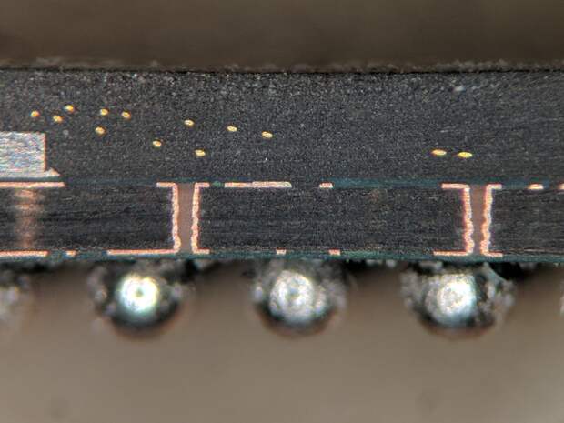
In some cases, flip chips connect directly to printed circuit boards using solder balls. In others, the die may be connected first to traces on a substrate, similar to an intermediate PCB, that then connects to the board itself. Traces on this intermediate layer connect the solder bumps from the die to the board connections. This allows for fanning-out connections on the die that would otherwise be too closely pitched for PCB connections.

While we may think of flip-chip technology as the new kid on the block, it’s actually been around for a long time. IBM pioneered the idea for discrete diodes and transistors in their mainframe computers of the 1960s, and it was later adapted for use in automobile electronics in the 1970s. Today, the technique is commonplace, and used in a wide variety of applications.
Not…
The post Flip Chips and Sunken Ships: Packaging Trick for Faster, Smaller Semiconductors appeared first on FeedBox.