Author: Al Williams / Source: Hackaday
ICs have certainly changed electronics, but how much do you really know about how they are built on the inside? While decapsulating and studying a modern CPU with 14 nanometer geometry is probably not a great first project, a simple 54HC00 logic gate is much larger and much easier to analyze, even at low magnification.
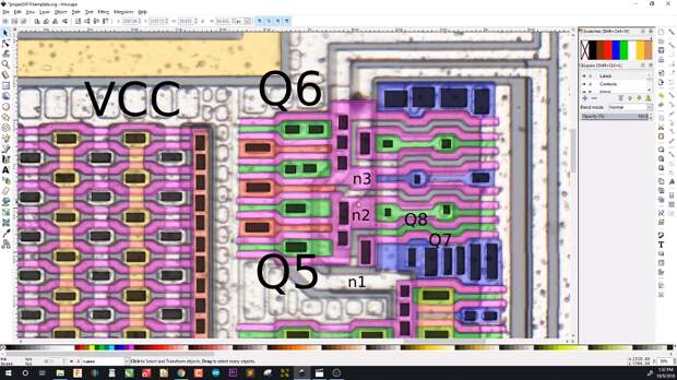
[Robert Baruch] took a die image of the chip and worked out what was going on, and shares his analysis in a recent video. You can see that video, below.The CMOS structures are simple because a MOSFET is so simple to make on an IC die. The single layer of aluminum conductors also makes things simple.
One disadvantage to working with a picture is you can’t etch off the passivation — the thin layer of glass over the top of the chip — and then remove the aluminum to see underneath. However, there isn’t much going on in a chip this simple and you can usually see outlines of contacts under the aluminum.
At this scale, it is possible to put the part under a microscope after…
The post Reverse Engineering CMOS appeared first on FeedBox.