Author: Brian Benchoff / Source: Hackaday

In recent months, the ability to hide components inside a circuit board has become an item of interest. We could trace this to the burgeoning badgelife movement, where engineers create beautiful works of electronic art. We can also attribute this interest to Bloomberg’s Big Hack, where Jordan Robertson and Michael Riley asserted Apple was the target of Chinese spying using components embedded inside a motherboard. The Big Hack story had legs, but so far no evidence of this hack’s existence has come to light, and the companies and governments involved have all issued denials that anything like this exists.
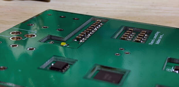
That said, embedding components inside a PCB is an interesting topic of discussion, and thanks to the dropping prices of PCB fabrication (this entire project cost $15 for the circuit boards), it’s now possible for hobbyists to experiment with the technique.
But first, it’s important to define what ‘stuffing components inside a piece of fiberglass’ is actually called. My research keeps coming back to the term ’embedded components’ which is utterly ungooglable, and a truly terrible name because ’embedded’ means something else entirely. You cannot call a PCB fabrication technique ’embedded components’ and expect people to find it on the Internet. For lack of a better term, I’m calling this ‘Oreo construction’, because of my predilection towards ‘stuf’, and because it needs to be called something. We’re all calling it ‘Oreo construction’ now, because the stuf is in the middle. This is how you do it with standard PCB design tools and cheap Chinese board houses.
Previous work

The immediate inspiration for this build comes from designer2k2 and a flat-pack Christmas ornament. This project used castellated pins and a series of holes to mount SMD parts to the side of a PCB instead of the top or bottom.
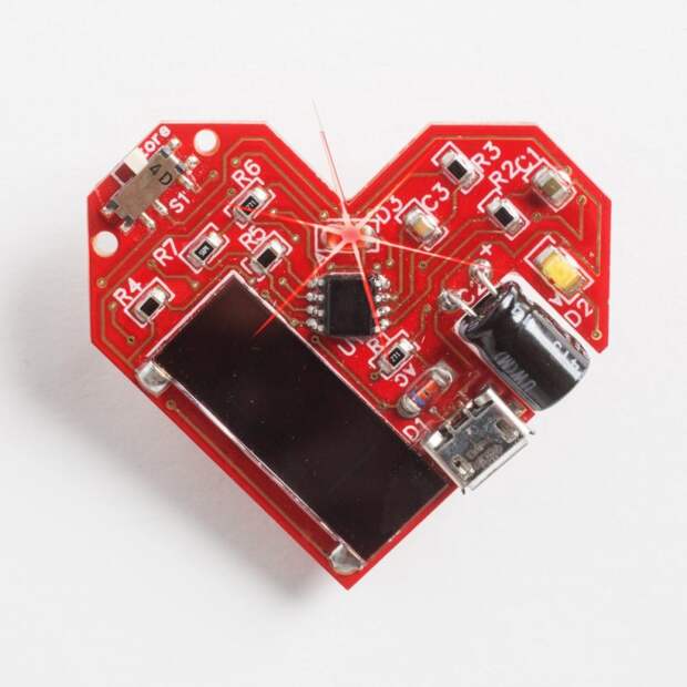
While soldering electronic components to the side of a PCB is somewhat novel, mounting electronic components to the side of a PCB is nothing new. Lumen Electronic Jewelry is producing a PCB ‘heart’ pin (right) with a capacitor and USB port mounted inside a cutout in the milling layer of a PCB. Likewise, other PCB projects — mostly PCB business cards — have experimented with mounting other components in a cutout in the milling layer. I have seen coin cell battery holders that use PCB cutouts with two ‘tabs’ that capture a battery between fiberglass.The idea of embedding components within a stack of fiberglass and copper is something we really haven’t seen before in the small-scale hobbyist world, but it can be done. Embedded components — there’s that ungooglable term again — can be done in very expensive products. The reasons for doing this range from saving physical space, better EMI shielding, and making something more difficult to reverse engineer. This is a technique for military and aerospace components, where price is no object.
Boards for military and aerospace work are one thing, but the past year saw a significant amount of discussion over embedded components, albeit for all the wrong reasons. Bloomberg’s Big Hack was a story about Supermicro motherboards shipped to Apple and Amazon that had additional components giving Chinese hackers a back door. This story was widely criticized, Apple and Amazon have fervently denied having found compromised motherboards, and any day now I’m expecting Supermicro to file suit in a libel case. This story did however generate a lot of discussion over how such a hack could happen. The top minds of the Twitterverse believe this could be done by embedding a small microcontroller inside the motherboard’s PCB, between the baseboard management controller and its Flash memory. This small microcontroller stuck between a few layers of PCB could in theory change a few bits of the BMC’s Flash to give attackers a back door, and Trammel Hudson gave an interesting talk at CCC discussing the theory of this fictional hack’s operation. It’s within the realm of possibility, but the smart money says this didn’t happen with Supermicro motherboards shipped to Amazon or Google. In any event, x-ray inspection or even a flying probe test would reveal any ’embedded component’ was in the PCB.
Layering Printed Circuit Board
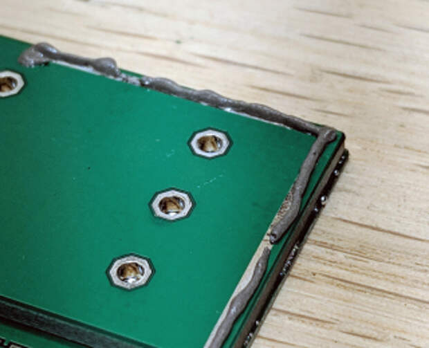
For this build, I have extended these techniques slightly by mechanically bonding the layers of PCBs together with solder. This was previously done by Voja Antonic and his work in building enclosures out of FR4. His approach was to create a strip of bare copper around the perimeter of each side of the enclosure. By mounting these sides of the enclosure at the correct angle, soldering the two flat planes of PCBs into a three dimensional shape is as simple as running a soldering iron over the exposed copper on the perimeter.


Each PCB in the stackup has exposed copper along the perimeter. By applying solder paste and clamping the boards together they’re read for reflow.
The post Oreo Construction: Hiding Your Components Inside The PCB appeared first on FeedBox.